Objective:
To study the
time response of a variety of simulated linear systems and to correlate the
studies with theoretical results.
Equipment
Description:
The setup has
been designed to provide a convenient means of studying the transient response
of linear systems. The block diagram and the function of each block is
described below:

Signal
sources:
There are three
built-in sources in the unit with the following nominal specifications:
Square wave: Frequency 40-90 Hz (variable)
:
Amplitude 0-2 Volt (p-p) (variable)
Triangular :
Frequency 40-90 Hz (variable)
: Amplitude 0-2 Volt (p-p) (variable)
Trigger :
Frequency 40-90 Hz (variable)
: Amplitude ± 5V (approx.)
Building
blocks:
A dynamic system
of desired configuration may be constructed by a suitable interconnection of
the basic blocks available. To avoid unnecessary complications, these blocks
are all pre-wired, they all have fixed transfer functions and handle signals
referred to a common ground.
- Error detector cum gain: The block has three inputs (e1, e2, e3) and one output (e0) which are related by the expression: e0= -K(e1+e2+e3) where K is the gain. The value of K may be varied from 0 to 10 by a ten turn potentiometer having a calibrated dial. This block may be used as simple error detector in a multiple loop system or simply as an adder.
- Integrator: The integrator block has an approximate transfer function of the form –K1/s and is used in simulating type-1 systems having a pole at the origin. Nominal value of K1 is 10.
- Time Constant: two time constant blocks in the system have transfer functions of the form –K2/ (sT+1) each. The second block has a X5 option which results in higher gain if necessary. Nominal values of K2=K3 and T1=T2 are 10 and 1msec respectively.
- Disturbance adder: this is two input (e1, e2) one output block (e0) having a defining equation of the form: e0= - (e1+e2). The block can have applications similar to the error detector.
- Amplifier: While completing the feedback path, one might need to invert the signal, for second order system, so that the resulting system is a negative feedback system. The amplifier here is a unity gain inverting amplifier used specifically for this purpose.
Apparatus
required:
DSO
Function generator
Pen drive of 4 GB or less/ trace sheet
Experimental work:
Some of the
experiments which may be performed on this unit are detailed below:
Open loop
response:
As a first step,
the open loop transfer function of all the blocks viz. integrator, time
constant, amplifier and error detector/adder are to be determined
experimentally. All measurements are done with the help of measuring DSO and
the signal source is in the built-in-square wave generator in each case. Save
at least two waveform in each experiment on the pen drive.
Error detector cum variable gain:
Apply a 100mV
square wave signal to any of the three inputs.
Set the gain
setting potentiometer to 10.0
Measure the p-p
output voltage and note its gain. Calculate the gain, this is the maximum value
of gain possible for this block.
Repeat for the
other two inputs one by one.
Disturbance adder (output):
This section may
be tested exactly in the same manner as error detector except that there are
only two inputs and there is no gain setting potentiometer.
Amplifier:
Apply a 1 V p-p
square wave input. Measure the p-p output voltage and notice its sign. Save the
waveform.
Integrator:
Apply 1V p-p
square wave input of known frequency. Measure the p-p output voltage of the
triangular wave and also notice its phase. Calculate the gain constant K of the
integrator.
Time constant:
Apply a 100mV
p-p square wave of known frequency. The frequency should be selected towards
the lower end. Find the time t=T at which the response reaches 63.2% from the
wave form. This is the time constant. Find the steady state value of the
response from the trace. The value of K is given by the ratio of p-p steady
state output to the p-p input amplitude.
Closed loop response:
First order system:
- There are two types of first order closed loop system can be formed, one using normal time constant and other using X5 time constant.
- Connect 1V p-p square wave signal to the REF point. Connect the output of gain to normal time constant. The output of time constant should be connected directly to the feedback node of the error detector.
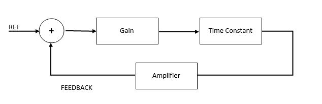 |
| First Order System |
- Connect one channel of DSO with REF point and other channel at time constant output.
- Vary the gain, and observe the effect at the output of time constant. Trace the wave forms and calculate maximum overshoot (MP), rise time (tr), peak time (tP), settling time (tS), delay time (td) and steady state error (eSS).
Table
1:
Sl. no
|
Gain (K)
|
MP
|
td
|
tr
|
tP
|
tS
|
eSS
|
Where
Maximum overshoot
(MP) = First peak value – Ref value
Delay time (td)
= that time when the response reaches 50% of the ref value.
Rise time (tr)
= that time when the response reaches 90% of the ref value.
Peak time (tP)
= that time when the response reaches its first peak value.
Settling time (tS)
= that time when the response comes 5% tolerance of ref value.
Steady state
error (eSS) = ref value – response at t(∞).
Repeat the above
steps for X5 time constant.
Second order type 0 system:
- Make the connection of the patch cord as per the block diagram shown below. Follow the same steps as above.
 |
| Second Order Type 0 |
- Observe all the effects and make the tabulation and save the wave forms.
- Try for time constant X5 also
Second order type 1 system:
- Make the connection of the patch cord as per the block diagram shown below. Follow the same steps as above.
 |
| Second Order Type 1 |
- Make the tabulation and save the wave forms.
- Try for time constant X5 also.
Disturbance Rejection:
- Connect the second order system as shown in the fig. below.
 |
| Second order System With Disturbance |
- Apply a low frequency disturbance signal (sinewave of 1 V) from function generator at N1 and see its effect on output. Save the wave form.
- Now apply the same disturbance signal at N2, and observe its effect on the output. Save the wave form and conclude the result.
No comments:
Post a Comment